ArC Instruments® delivers high performance testing platforms for characterizing ‘en masse’ novel technologies in a fast and automated fashion.
ArC ONE® is specifically designed for working with emerging 2-terminal nanoelectronic memory devices. The instrument is controlled through a simple yet powerful user interface that allows for ArC ONE® capabilities to be broadly accessible, from research students to competent test engineers.
ArC ONE® can effortlessly be integrated into any R&D setting to accelerate discovery. It can be used with any prober for accessing from single up to 1024 devices directly on wafer or even be used as a stand-alone portable testing capability to enable advanced in-situ physicochemical characterisation techniques.
And while this instrument provides unrivalled versatility in testing, it does so without compromising on performance; delivering nanosecond pulsing and other bespoke state-of-art capabilities that are essential for characterising advanced memory devices.
This guide covers the installation of this apparatus and details its capabilities.
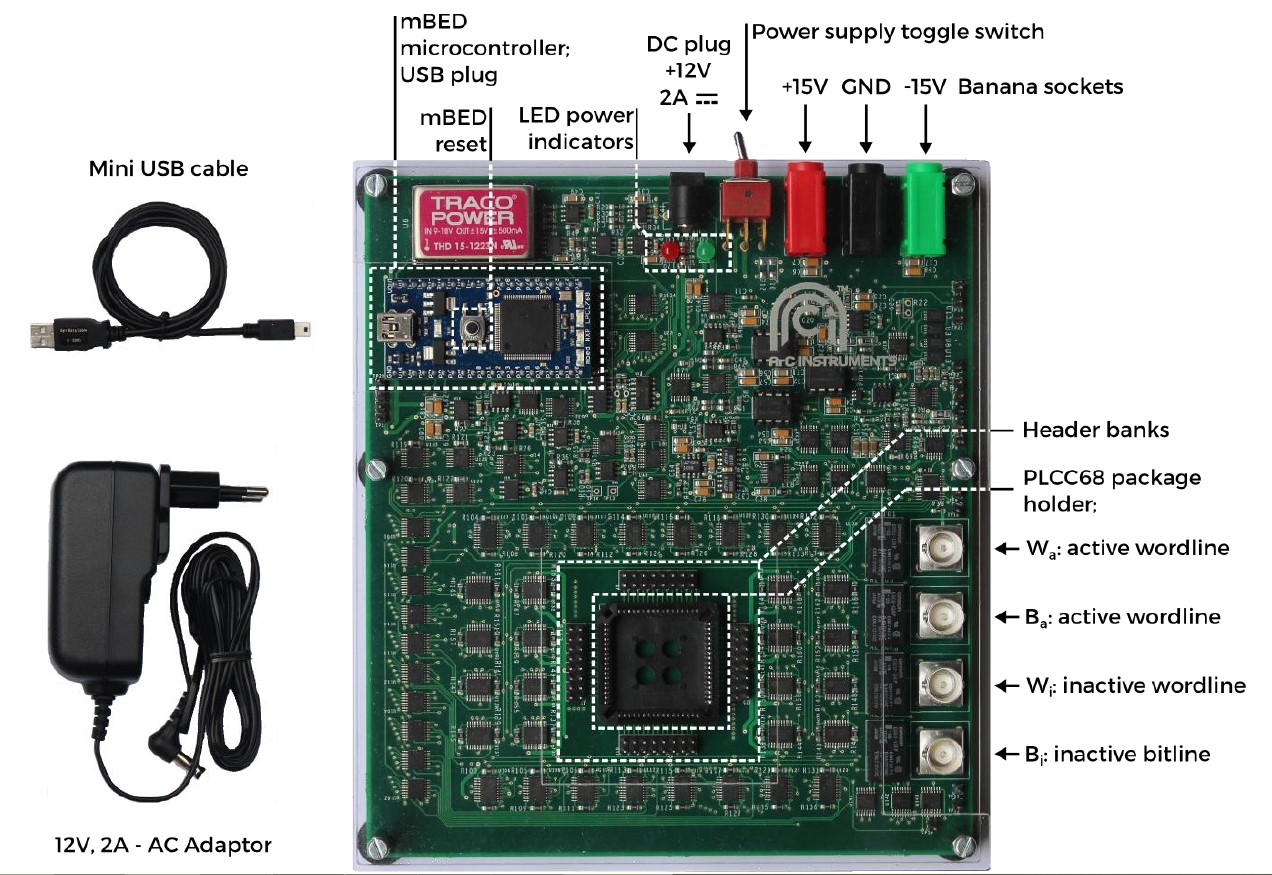
The ArC ONE® system consists of a hardware instrumentation board (ArC ONE®) and a dedicated software graphical user interface – GUI (ArC ONE Control®) The hardware and adjacent components straight out of the box are illustrated below
To power up the board, either plug in the provided AC power adaptor in the DC plug, or connect a desktop power supply to the banana sockets. Toggle the power supply switch towards the required power supply input. The red and green LEDs should turn on, indicating the board is powered. For best results, utilise a battery supply.
The PLCC socket holds packaged samples. The socket accepts 68-pin ceramic quad flat pack chip carriers (CQFJ). Typical cavity sizes for these packages are (in inches) 0.265×0.265, 0.3×0.3, 0.4×0.4 and 0.46×0.46. Its pin map is illustrated below in Figure 2.
In the case where devices need to be accessed away from the board, (eg via a probe card to solid-state devices on wafer), the surrounding headers provide access to individual word- and bitline addresses.

To install the ArC ONE® Control GUI, follow the steps below: (for Windows 7 and above)
To update the ArC ONE® Control GUI suite, first start the interface, make sure the ArC ONE® board is connected via USB and look for the Platform Manager launch button on the top left corner of the GUI. An internet connection is required for this feature.
If the button is active, then an update is available. Click the button to start the automatic updater. You can manually check for updates at Settings » Check for updates.
The ArC ONE® Control GUI is distributed under the General Public License (GNU) Version 3. It is therefore an open-source copy, allowing any user to modify and re-utilise its contents, as long as the original creator is mentioned. Keep a copy of the initial source file to ensure the operation of the ArC® platform.
The ArC GUI allows easy control of the ArC ONE® platform. It is divided into a number of functional panels:
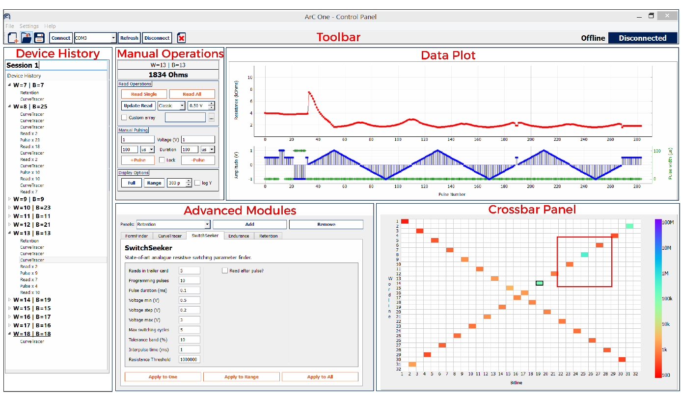
Toolbar: contains buttons for saving data, creating, opening and clearing a session, ArC ONE® connection management as well as a GUI session mode indicator (refer to Section 3.3) and an ArC ONE® connection indicator, on the right hand side. File menu contains Save, Open, Clear and Exit options. Settings menu allows the user to modify hardware settings and choose a new working directory on the fly. Help menu shows the documentation (this file), and ArC Instruments Ltd. contact information.
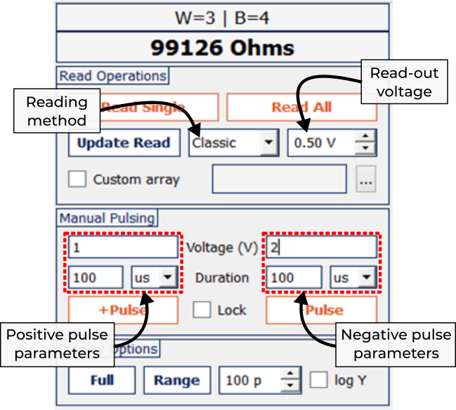
Manual Operations panel: Contains buttons for reading a single selected cell or the full array. The Custom Array checkbox restricts the crossbar active devices to any combination of devices in a 32×32 array, based on a text file. The read type can be changed via the drop down menu. The reading voltage can also be set via the input text field. Clicking ‘Update’ updates the reading method on the ArC ONE® board. Manual pulsing of 0 to ±12V and down to 90ns can be applied on the selected device by pressing +Pulse (positive pulse) or -Pulse (negative pulse). Separate input fields allow for independent setting of positive and negative pulsing polarities.
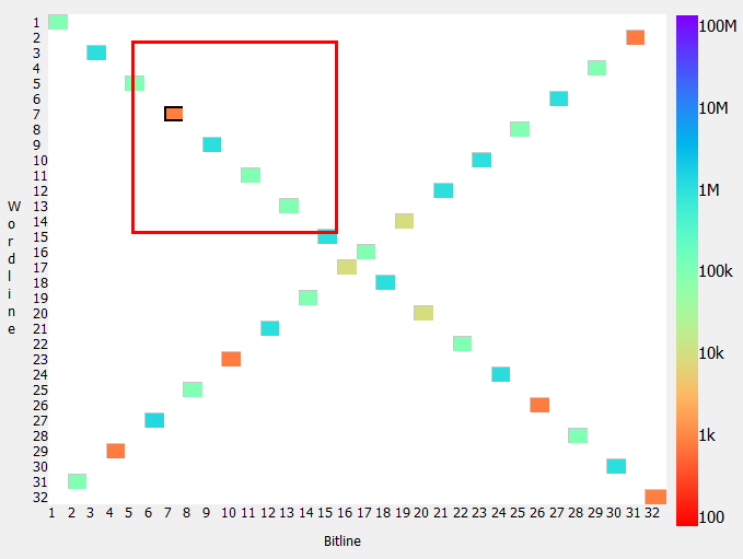
Crossbar Panel: Direct selection of individual devices is performed by left clicking the required position. The selected crosspoint is highlighted by a thick black outline and represents the current device under test (DUT) for any further operation. The resistive state of each device is represented by the colour of the cell, and the colour coding is illustrated at the right of the crossbar. Hovering over a cross-point reveals the absolute resistance value of the last read operation. Additionally, left clicking and dragging allows selection of a square region of devices in a crossbar if local testing is required.
Data Plot panel: Top plot shows the resistive state evolution of a device. Bottom plot shows the pulse amplitude and pulse duration per pulse number in chronological order. During the application of an automated pulsing script, the plot is updated live with incoming measurement data.
Device History panel: Contains the pulsing history for each device in the crossbar, if any is available. History entries can be accessed to display additional measurement results.
Pulsing Modules panel: The drop-down menu contains a number of custom pulsing scripts, and selecting one displays its corresponding options which the user can then set. Panels include custom device operation scripts such as FormFinder, SwitchSeeker, standard IV measurement protocols such as CurveTracer, and memristor specific characterisation pulsing scripts such as Endurance and Retention. The pulsing scripts are described in detail in Section 3.5.
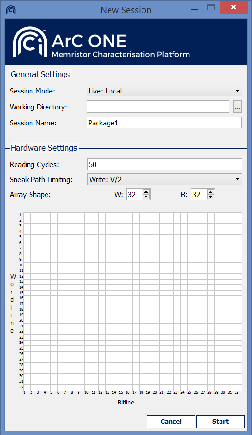
On starting the GUI, the window on the right below will appear which allows setting up a new measurement session. There are 2 main setting categories:
General settings
The Session Mode dropdown selects the operating mode of the system and four options:
[W=1, B=1]. WARNING: Please
ensure no package is connected in the PLCC68 holder or through the
header bank.Working Directory entry allows the user to choose the directory in which measurement sessions will be saved. Press the browse button on the right of the entry to navigate. This can be setup later as well.
Session Name entry sets the name of the session.


Hardware settings
Reading Cycles: Every test device resistive state
READ measurement is by default an average of n recorded
data points. This entry sets the value of n. A higher
number translates into a slower, but more accurate measurement.
n=50 is a reasonable, general purpose choice.
Sneak Path Limiting sets up the sneak path mitigation technique employed in selectorless crossbar arrays. The user can choose between V/2, V/3. The following table illustrates how the bias voltage, Vw, is applied across different devices in the two sneak path mitigation scenarios.
| Node | V/2 option | V/3 option |
|---|---|---|
| Active wordline | Vw | Vw |
| Active bitline | GND | GND |
| Inactive wordline | Vw/2 | Vw/3 |
| Inactive bitline | Vw/2 | Vw/3 |
Array Shape counters set up the size of the array. Any size is selectable between 1 and 32 word- and bitlines.
After the new session has been set up, the right hand side of the toolbar should indicate the session mode, and the connection status showing Disconnected as below.

Make sure ArC ONE® is connected to the PC via a USB cable, and the board is powered up. A blue LED on the on-board mBED indicates the board is connected to the PC, and red and green LEDs indicate the board is powered up.

From the toolbar (above), select the corresponding COM port of the ArC ONE® board. If you don’t know it, you can find it in Windows by going to:
COM and LTP)
and expand;COMX), and make a note of the COM port number.Return to the GUI and select the respective COM port from the dropdown list, and click Connect. If the port is not there, click Refresh and wait for up to 10 seconds. The port should now appear.
Once the connection is successful, the connection status will turn green like below:

If any connection problems occur, please refer to Section 5 of this manual.
Many basic operations such as reading and writing, as well as data display and device history visualisation are available at a click of a button. As a general rule of thumb, the buttons coloured in orange perform invasive operations on the selected device, or range of devices. Buttons coloured in dark blue perform non-invasive operations, such as updating ArC ONE® settings or managing data display options.
Left click the required device on the Crossbar Panel to select it. The device will be highlighted by a black outline. Any following invasive operation will be performed on that device.
Hovering the mouse over a crossbar device shows address and resistance information in the small floating information panel.
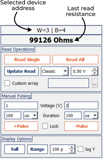
The address of the currently selected device appears on top of the Manual Operations panel, along with its corresponding last measured value of resistance.
Left click and drag in order to select a range of devices. A box with a thick red outline will indicate the selected sub-array. Right click anywhere on the Crossbar Panel to toggle the visibility of the box.
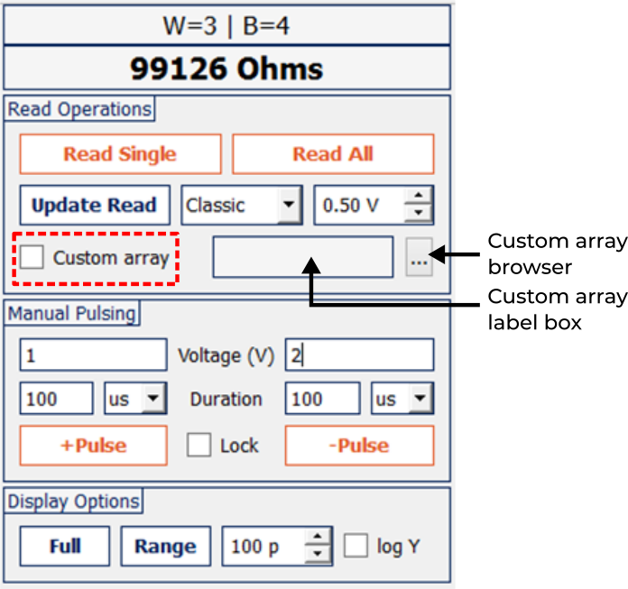
If only a particular set of crosspoints is required for a measurement
session, these can be selected on the interface via checking the
Custom Array checkbox. A file open dialogue will appear
which allows the user to select a text file containing the required
addresses. The file should contain the word- and bitlines of the
devices separated by a single comma character “,” one pair
per line.
The same open file dialogue will appear if the browse array file button is pressed. The set of device addresses are then highlighted in the Crossbar Panel, while the others are hidden. Any device select, or device operation will be constrained to this set. The devices within the range selected by left clicking and dragging will constitute the target area for any operations carried out via the Apply to Range directive.
In the Read Operations sub-panel, click Read Single to perform one READ operation on the selected device (highlighted in the Crossbar Panel, and listed on top of the Manual Operations panel). The new value of resistance is updated there. The Data Plot panel will be updated with the new measurement. Click Read All to read all devices in the crossbar.
Update Read updates the reading method on the ArC board. Select the reading method between the following read-out modes:
Select the reading voltage by left-clicking the up and down arrows in the reading voltage counter, or introducing a float number by hand. Remember to click Update Read every time the reading method, or reading voltage is changed.


In the Manual Pulsing sub-panel, single WRITE pulses can be applied on a selected device.
Click the +Pulse to immediately apply a positive voltage pulse, and –Pulse to apply a negative pulse. The parameters of the pulse, such as amplitude and duration, can be changed via the entry fields above the corresponding buttons.
A READ operation is automatically performed after each manual pulse. The new measurement is added in the Data Plot panel, along with the applied manual pulse.
Checking the Lock checkbox disables the negative pulse parameter entry fields. Clicking –Pulse will then apply a negative pulse with the parameters of the positive pulse entry fields. For example: positive pulse parameters are 1 V at 100 ms, negative pulse parameters are 2 V at 1 ms. Clicking +Pulse will apply 1 V at 100 ms, -Pulse will apply 2 V at 1 ms. After checking the Lock checkbox, clicking +Pulse will apply 1 V at 100 ms, and –Pulse will apply -1 V at 100 ms.
In the Display Options sub-panel, the user can modify the plot options in the Data Plot panel.
Press Full to display all recorded data points for the selected device. Press Range to display the last X number of points, where X is set in the adjacent counter. Tick the log Y checkbox to set logarithmic Y axis in the top subplot of the Data Plot panel.
The data plot panel is separated into two subplots as shown in the following figure.
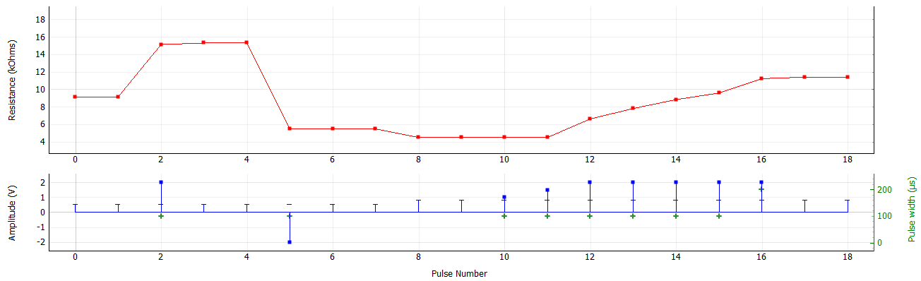
Top subplot shows read value of resistance at each pulse number. Bottom subplot shows:
For example, in figure 14 at pulse #1, the resistance is read at 0.5 V as ~9 kΩ. Next, a 2 V, 100 µs voltage pulse is applied shown at pulse #2. The resistance is then automatically read as 15 kΩ, also at 0.5 V, indicated by the blue horizontal line marker at the same pulse #2. Therefore, a 2 V, 100 µs voltage pulse has changed the resistance of the device as read at 0.5 V, from 9 kΩ to 15 kΩ.
By default the data plot panel shows resistance values. This can be changed to either conductance, current or absolute current from the main toolbar.

Additional display options, such as setting custom x and
y-axis range, or exporting the figure image files can be
accessed by right clicking on the Data Plot panel.
All invasive device operations are logged in the Device History panel on left hand side of the interface. Device addresses are added from top to bottom in a chronological order following any operation. The last device address where an operation was performed is underlined. Selecting a device address from the Device History panel will also select and display its pulsing history in the Data Plot panel.
Single device operations are listed below its corresponding address from top to bottom in a chronological order. These become visible by clicking the dropdown marker.
READ operations are tagged with Read x N, where
N is the number of read pulses applied in sequence. WRITE
operations are tagged with Pulse x N, where N
is the number of manual WRITE pulses applied in sequence.
Advanced pulsing algorithms are tagged with their corresponding name. Double clicking some advanced pulsing algorithm entries displays further measurement results. For example, following a CurveTracer measurement, double clicking the “CurveTracer” history entry will display the resulting IV curve. See Section 3.5 for more information.
All raw data is saved in standard .csv files by clicking
the save button in the toolbar. Every READ or WRITE operation is
represented as a line entry in this file, following the format below
Wordline, Bitline, Resistance, Amplitude, Pulse Width, Tag, ReadTag, Read Voltage
Wordline and
Bitline: target device address.Resistance: last read resistance of
target device.Amplitude: pulse amplitude of
operation.Tag: type of operation and additional
information.ReadTag: represents the read type
employed for the READ operation. Its format is RX where
X is a unique code for the read type.ReadVoltage: read voltage used for the
READ operation (if any).The Tag field is of special importance as it identifies
the type of operation. Manual read and pulse operations use the
following conventions
| Tag | Description | Comments |
|---|---|---|
F RX V=Vr |
A Read All
operation. X represents the read type 0:
Classic; 1: TIA; 2: TIA4P. Vr is
the read-out voltage. |
Data points are not visible in the Device
History panel. Vr is saved in the Amplitude
column and PulseWidth is always 0. |
S RX V=Vr |
A Read Single
operation. X and Vr as above. |
Data point is visible in the Device
History panel. PulseWidth is always 0. |
P |
Singular pulses when using the ±Pulse buttons in the Manual Operations panel. | Resistance is the resistance
of the device upon a read-out immediately after the pulse. |
All other pulsing modules use the TAG_x format.
TAG is a unique identifier assigned to each module. For
instance CurveTracer uses the CT tag, Retention uses the
RET tag and so on. The x part is a single
character either s, i or e;
s signals the start of the operation and
e the end. All intermediate points are
assigned the i character. Additional information for each
module is provided in their respective sections. Depending on the
module, additional information may be provided in the
Tag.
The following plot illustrates a set of operation performed on the device with word- and bitline coordinates 15 and 15 respectively. The resulting dataset is also presented below.
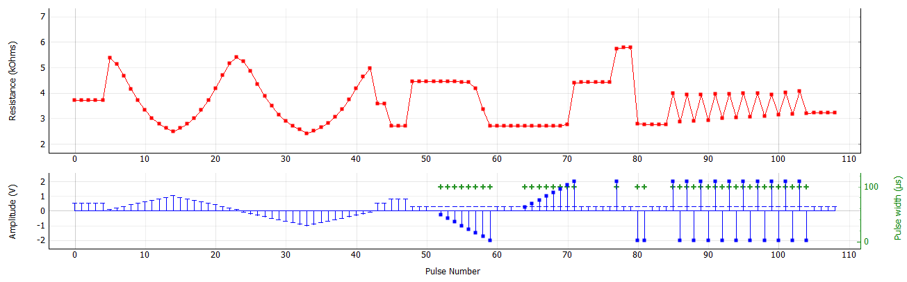
| # | Word | Bit | Res. (Ω) | Ampl. (V) | Pulse (s) | Tag | ReadTag | Vr (V) |
|---|---|---|---|---|---|---|---|---|
| 0 | 15 | 15 | 3710.626 | 0.5 | 0 | S R2 V=0.5 | R2 | 0.5 |
| 1 | 15 | 15 | 3709.371 | 0.5 | 0 | S R2 V=0.5 | R2 | 0.5 |
| 2 | 15 | 15 | 3711.800 | 0.5 | 0 | S R2 V=0.5 | R2 | 0.5 |
| 3 | 15 | 15 | 3711.342 | 0.5 | 0 | S R2 V=0.5 | R2 | 0.5 |
| 4 | 15 | 15 | 3712.748 | 0.5 | 0 | S R2 V=0.5 | R2 | 0.5 |
| 5 | 15 | 15 | 5387.196 | 0.095865 | 0 | CT_s | R2 | 0.095865 |
| 6 | 15 | 15 | 5132.203 | 0.197452 | 0 | CT_i_1 | R2 | 0.197452 |
| 7 | 15 | 15 | 4678.331 | 0.298781 | 0 | CT_i_1 | R2 | 0.298781 |
| 8 | 15 | 15 | 4168.121 | 0.399095 | 0 | CT_i_1 | R2 | 0.399095 |
| 9 | 15 | 15 | 3710.786 | 0.498812 | 0 | CT_i_1 | R2 | 0.498812 |
| 10 | 15 | 15 | 3329.797 | 0.601575 | 0 | CT_i_1 | R2 | 0.601575 |
| 11 | 15 | 15 | 3015.440 | 0.706225 | 0 | CT_i_1 | R2 | 0.706225 |
| 12 | 15 | 15 | 2788.292 | 0.810664 | 0 | CT_i_1 | R2 | 0.810664 |
| 13 | 15 | 15 | 2623.501 | 0.912557 | 0 | CT_i_1 | R2 | 0.912557 |
| 14 | 15 | 15 | 2490.076 | 1.014837 | 0 | CT_i_1 | R2 | 1.014837 |
| 15 | 15 | 15 | 2621.308 | 0.912573 | 0 | CT_i_1 | R2 | 0.912573 |
| 16 | 15 | 15 | 2789.779 | 0.810455 | 0 | CT_i_1 | R2 | 0.810455 |
| 17 | 15 | 15 | 3020.242 | 0.706225 | 0 | CT_i_1 | R2 | 0.706225 |
| 18 | 15 | 15 | 3331.286 | 0.601511 | 0 | CT_i_1 | R2 | 0.601511 |
| 19 | 15 | 15 | 3720.155 | 0.498795 | 0 | CT_i_1 | R2 | 0.498795 |
| 20 | 15 | 15 | 4177.835 | 0.398998 | 0 | CT_i_1 | R2 | 0.398998 |
| 21 | 15 | 15 | 4687.421 | 0.298636 | 0 | CT_i_1 | R2 | 0.298636 |
| 22 | 15 | 15 | 5160.943 | 0.197452 | 0 | CT_i_1 | R2 | 0.197452 |
| 23 | 15 | 15 | 5411.013 | 0.095865 | 0 | CT_i_1 | R2 | 0.095865 |
| 24 | 15 | 15 | 5234.892 | -0.09978 | 0 | CT_i_1 | R2 | -0.09978 |
| 25 | 15 | 15 | 4851.898 | -0.20206 | 0 | CT_i_1 | R2 | -0.20206 |
| 26 | 15 | 15 | 4356.187 | -0.30347 | 0 | CT_i_1 | R2 | -0.30347 |
| 27 | 15 | 15 | 3871.069 | -0.40329 | 0 | CT_i_1 | R2 | -0.40329 |
| 28 | 15 | 15 | 3491.388 | -0.5044 | 0 | CT_i_1 | R2 | -0.5044 |
| 29 | 15 | 15 | 3146.329 | -0.60612 | 0 | CT_i_1 | R2 | -0.60612 |
| 30 | 15 | 15 | 2899.183 | -0.70682 | 0 | CT_i_1 | R2 | -0.70682 |
| 31 | 15 | 15 | 2710.133 | -0.8068 | 0 | CT_i_1 | R2 | -0.8068 |
| 32 | 15 | 15 | 2563.161 | -0.90872 | 0 | CT_i_1 | R2 | -0.90872 |
| 33 | 15 | 15 | 2415.091 | -1.01092 | 0 | CT_i_1 | R2 | -1.01092 |
| 34 | 15 | 15 | 2515.301 | -0.9085 | 0 | CT_i_1 | R2 | -0.9085 |
| 35 | 15 | 15 | 2652.484 | -0.80683 | 0 | CT_i_1 | R2 | -0.80683 |
| 36 | 15 | 15 | 2830.457 | -0.70664 | 0 | CT_i_1 | R2 | -0.70664 |
| 37 | 15 | 15 | 3060.042 | -0.60627 | 0 | CT_i_1 | R2 | -0.60627 |
| 38 | 15 | 15 | 3369.232 | -0.50439 | 0 | CT_i_1 | R2 | -0.50439 |
| 39 | 15 | 15 | 3738.675 | -0.40321 | 0 | CT_i_1 | R2 | -0.40321 |
| 40 | 15 | 15 | 4194.151 | -0.3035 | 0 | CT_i_1 | R2 | -0.3035 |
| 41 | 15 | 15 | 4640.740 | -0.20174 | 0 | CT_i_1 | R2 | -0.20174 |
| 42 | 15 | 15 | 4973.099 | -0.09959 | 0 | CT_e | R2 | -0.09959 |
| 43 | 15 | 15 | 3578.096 | 0.5 | 0 | S R2 V=0.5 | R2 | 0.5 |
| 44 | 15 | 15 | 3580.594 | 0.5 | 0 | S R2 V=0.5 | R2 | 0.5 |
| 45 | 15 | 15 | 2714.075 | 0.8 | 0 | S R2 V=0.8 | R2 | 0.8 |
| 46 | 15 | 15 | 2715.643 | 0.8 | 0 | S R2 V=0.8 | R2 | 0.8 |
| 47 | 15 | 15 | 2715.713 | 0.8 | 0 | S R2 V=0.8 | R2 | 0.8 |
| 48 | 15 | 15 | 4449.561 | 0.3 | 0 | S R2 V=0.3 | R2 | 0.3 |
| 49 | 15 | 15 | 4454.619 | 0.3 | 0 | S R2 V=0.3 | R2 | 0.3 |
| 50 | 15 | 15 | 4454.496 | 0.3 | 0 | S R2 V=0.3 | R2 | 0.3 |
| 51 | 15 | 15 | 4453.649 | 0 | 0 | FF_s | R2 | 0.3 |
| 52 | 15 | 15 | 4455.347 | -0.25 | 0.0001 | FF_i | R2 | 0.3 |
| 53 | 15 | 15 | 4450.094 | -0.5 | 0.0001 | FF_i | R2 | 0.3 |
| 54 | 15 | 15 | 4448.665 | -0.75 | 0.0001 | FF_i | R2 | 0.3 |
| 55 | 15 | 15 | 4437.407 | -1 | 0.0001 | FF_i | R2 | 0.3 |
| 56 | 15 | 15 | 4420.111 | -1.25 | 0.0001 | FF_i | R2 | 0.3 |
| 57 | 15 | 15 | 4171.116 | -1.5 | 0.0001 | FF_i | R2 | 0.3 |
| 58 | 15 | 15 | 3355.073 | -1.75 | 0.0001 | FF_i | R2 | 0.3 |
| 59 | 15 | 15 | 2714.420 | -2 | 0.0001 | FF_e | R2 | 0.3 |
| 60 | 15 | 15 | 2717.500 | 0.3 | 0 | S R2 V=0.3 | R2 | 0.3 |
| 61 | 15 | 15 | 2717.707 | 0.3 | 0 | S R2 V=0.3 | R2 | 0.3 |
| 62 | 15 | 15 | 2717.669 | 0.3 | 0 | S R2 V=0.3 | R2 | 0.3 |
| 63 | 15 | 15 | 2717.591 | 0 | 0 | FF_s | R2 | 0.3 |
| 64 | 15 | 15 | 2719.074 | 0.25 | 0.0001 | FF_i | R2 | 0.3 |
| 65 | 15 | 15 | 2718.968 | 0.5 | 0.0001 | FF_i | R2 | 0.3 |
| 66 | 15 | 15 | 2716.181 | 0.75 | 0.0001 | FF_i | R2 | 0.3 |
| 67 | 15 | 15 | 2715.721 | 1 | 0.0001 | FF_i | R2 | 0.3 |
| 68 | 15 | 15 | 2713.022 | 1.25 | 0.0001 | FF_i | R2 | 0.3 |
| 69 | 15 | 15 | 2713.360 | 1.5 | 0.0001 | FF_i | R2 | 0.3 |
| 70 | 15 | 15 | 2776.728 | 1.75 | 0.0001 | FF_i | R2 | 0.3 |
| 71 | 15 | 15 | 4390.111 | 2 | 0.0001 | FF_e | R2 | 0.3 |
| 72 | 15 | 15 | 4414.533 | 0.3 | 0 | S R2 V=0.3 | R2 | 0.3 |
| 73 | 15 | 15 | 4420.807 | 0.3 | 0 | S R2 V=0.3 | R2 | 0.3 |
| 74 | 15 | 15 | 4421.931 | 0.3 | 0 | S R2 V=0.3 | R2 | 0.3 |
| 75 | 15 | 15 | 4438.629 | 0.3 | 0 | S R2 V=0.3 | R2 | 0.3 |
| 76 | 15 | 15 | 4437.45 | 0.3 | 0 | S R2 V=0.3 | R2 | 0.3 |
| 77 | 15 | 15 | 5745 | 2 | 1.0E-04 | P | R2 | 0.3 |
| 78 | 15 | 15 | 5791.744 | 0.3 | 0 | S R2 V=0.3 | R2 | 0.3 |
| 79 | 15 | 15 | 5794.007 | 0.3 | 0 | S R2 V=0.3 | R2 | 0.3 |
| 80 | 15 | 15 | 2802 | -2 | 1.0E-04 | P | R2 | 0.3 |
| 81 | 15 | 15 | 2759 | -2 | 1.0E-04 | P | R2 | 0.3 |
| 82 | 15 | 15 | 2763.08 | 0.3 | 0 | S R2 V=0.3 | R2 | 0.3 |
| 83 | 15 | 15 | 2761.165 | 0.3 | 0 | S R2 V=0.3 | R2 | 0.3 |
| 84 | 15 | 15 | 2762.447 | 0.3 | 0 | S R2 V=0.3 | R2 | 0.3 |
| 85 | 15 | 15 | 3999.051 | 2 | 0.0001 | EN_s | R2 | 0.3 |
| 86 | 15 | 15 | 2861.266 | -2 | 0.0001 | EN_i | R2 | 0.3 |
| 87 | 15 | 15 | 3936.899 | 2 | 0.0001 | EN_i | R2 | 0.3 |
| 88 | 15 | 15 | 2888.566 | -2 | 0.0001 | EN_i | R2 | 0.3 |
| 89 | 15 | 15 | 3927.748 | 2 | 0.0001 | EN_i | R2 | 0.3 |
| 90 | 15 | 15 | 2935.807 | -2 | 0.0001 | EN_i | R2 | 0.3 |
| 91 | 15 | 15 | 3960.851 | 2 | 0.0001 | EN_i | R2 | 0.3 |
| 92 | 15 | 15 | 3010.295 | -2 | 0.0001 | EN_i | R2 | 0.3 |
| 93 | 15 | 15 | 3975.576 | 2 | 0.0001 | EN_i | R2 | 0.3 |
| 94 | 15 | 15 | 3030.883 | -2 | 0.0001 | EN_i | R2 | 0.3 |
| 95 | 15 | 15 | 4004.491 | 2 | 0.0001 | EN_i | R2 | 0.3 |
| 96 | 15 | 15 | 3069.084 | -2 | 0.0001 | EN_i | R2 | 0.3 |
| 97 | 15 | 15 | 3993.906 | 2 | 0.0001 | EN_i | R2 | 0.3 |
| 98 | 15 | 15 | 3098.52 | -2 | 0.0001 | EN_i | R2 | 0.3 |
| 99 | 15 | 15 | 3931.544 | 2 | 0.0001 | EN_i | R2 | 0.3 |
| 100 | 15 | 15 | 3140.177 | -2 | 0.0001 | EN_i | R2 | 0.3 |
| 101 | 15 | 15 | 4010.678 | 2 | 0.0001 | EN_i | R2 | 0.3 |
| 102 | 15 | 15 | 3161.425 | -2 | 0.0001 | EN_i | R2 | 0.3 |
| 103 | 15 | 15 | 4076.823 | 2 | 0.0001 | EN_i | R2 | 0.3 |
| 104 | 15 | 15 | 3209.966 | -2 | 0.0001 | EN_e | R2 | 0.3 |
| 105 | 15 | 15 | 3215.763 | 0.3 | 0 | S R2 V=0.3 | R2 | 0.3 |
| 106 | 15 | 15 | 3215.978 | 0.3 | 0 | S R2 V=0.3 | R2 | 0.3 |
| 107 | 15 | 15 | 3216.013 | 0.3 | 0 | S R2 V=0.3 | R2 | 0.3 |
| 108 | 15 | 15 | 3215.842 | 0.3 | 0 | S R2 V=0.3 | R2 | 0.3 |
In addition to the manual operations there are several advanced pulsing scripts available from the Pulsing Modules panel.
Pulsing modules can be enabled by selecting a module from the Panels field and clicking the Add button. Modules are independent so multiple copies can be enabled at the same time with different biasing parameters. Similarly the active panel can be removed by clicking the Remove button. Panel parameters can be saved and recalled later using the Save and Load buttons. Loading a set of modules parameters from file will not overwrite your active modules but append it as a new tab.
The active module can be applied to selected device, range of devices all the whole crossbar by using the buttons Apply to One, Apply to Range or Apply to All respectively. Please note that applying a module to multiple devices might not be available or not behaving as expected depending on the functionality of the module. Refer to the documentation of each module for more details.
FormFinder is a versatile pulsing algorithm which applies a pulsed voltage ramp with an option of two stop conditions. After each WRITE pulse, a READ pulse is applied by default. A summary of the operation of this module can be seen in the figure below.

The following parameters are used for this module. A standard pulsed voltage ramp, with one pulse per step can be achieved by setting Nr of pulses to 1, and making Pulse width min (μs) and Pulse width max (μs) equal to the desired pulse width value.
| Parameter | Description |
|---|---|
| Voltage min (V) | Initial voltage of the ramp. |
| Voltage step (V) | ΔV between subsequent voltage steps. |
| Voltage max (V) | Maximum voltage of the ramp; also acts as stop condition. |
| Pulse width min (μs) | Minimum pulse width that is used. |
| Pulse width step | Pulse width increment for each subsequent step. This can be either in % of the previous step or a fixed step in μs (see Pulse progression below). |
| Pulse width max (μs) | Maximum pulse width. |
| Interpulse time (ms) | Delay between two subsequent WRITE pulses. |
| Nr of pulses | Number of WRITE pulses per step. |
| Resistance threshold (Ω) | Halts the ramp when resistance drops below this value. Use 0 to disable. |
| Resistance threshold (%) | Same as above but as percentage of initial resistance. Only used when Rthr is checked. |
| pSR | Series resistance: 1: 1 kΩ;
2: 10 kΩ; 3: 100 kΩ; 4: 1 MΩ;
7: disabled. |
| Negative amplitude | Check this to invert the polarity of the above voltages. |
| Use Rthr (%) | Enable the use of percentage-based thresholds |
| Pulse progression | Use multiplicative (%-based) or linear (fixed step) increments for pulse widths. |
Tag: FF. FormFinder follows the
standard FF_{s,i,e} format.
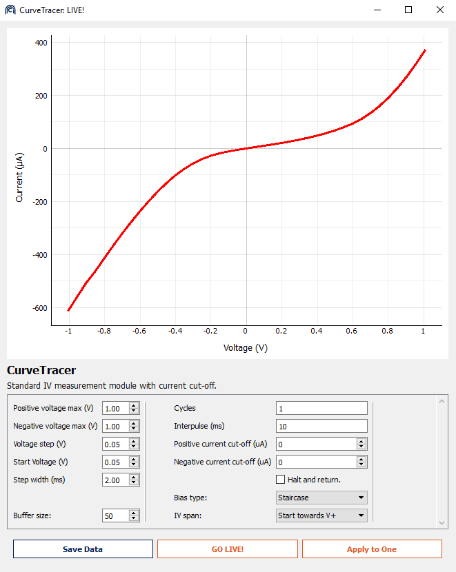
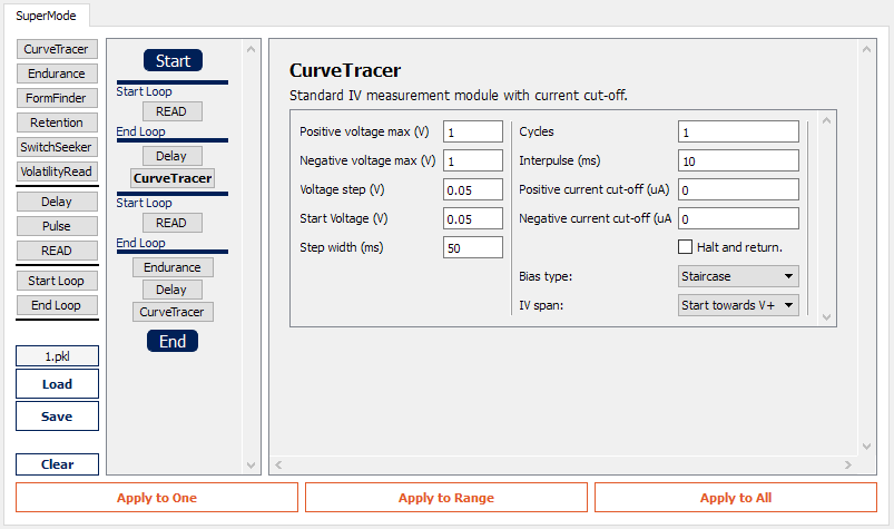
CurveTracer is a standard triangular pulsed IV measurement module, with incorporated current cut-off. During each WRITE pulse, a current measurement is taken towards the end of the pulse.

| Parameter | Description |
|---|---|
| Positive Vmax (V) | Maximum positive voltage. |
| Negative Vmax (V) | Maximum negative voltage. |
| Voltage step (V) | Voltage step for both polarities. |
| Start voltage (V) | Initial voltage for both polarities (min: 50 mV). |
| Step width (ms) | Hold time (or pulse width) of each voltage step (min: 1 ms). |
| Cycles | Number of consecutive I-Vs to be acquired. |
| Interpulse time (ms) | Delay between adjacent pulses (only for Pulsed bias type). |
| Positive cutoff (μA) | Positive compliance current (min: 10 μA max: 1000 μA). Set 0 to disable compliance. |
| Negative cutoff (μA) | Negative compliance current (min: 10 μA max: 1000 μA). Set 0 to disable compliance. |
| Halt and Return | When checked the applied bias will be cut-off within 30 μs and return to 0 if current threshold has been exceeded (if >0 μA). |
| Bias type | Staircase mode set interpulse to 0 ms. In pulsed mode device bias is set to 0 V for the duration of interpulse time. |
| IV span | Different sweep modes. Only V± restricts the I-V sweep to that particular polarity. Start towards V± selects the initial polarity when sweeping both positive and negative voltages. |
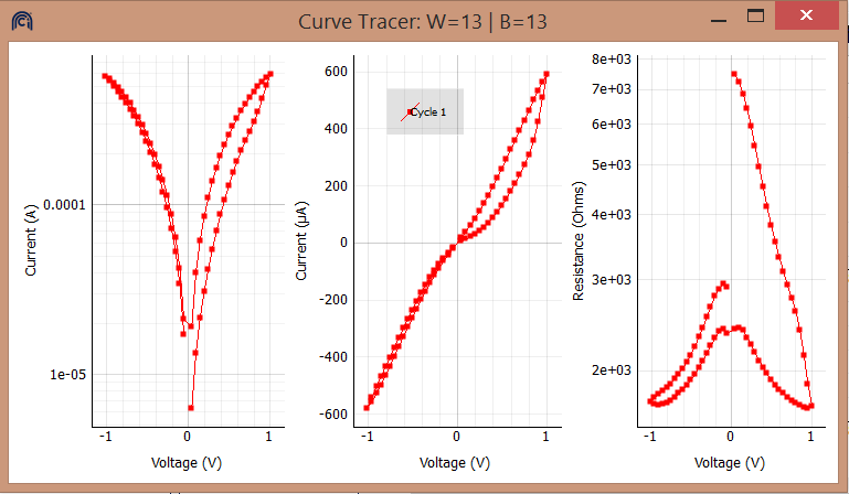
Following application of the protocol a “CurveTracer” entry will appear in the Device History panel. Double click it to visualize the I-V measurement as shown in fig. 18. Right click on the plots and select Export to save the figure, or corresponding data.
Pressing the LIVE button opens up a panel similar to CurveTracer (fig. 19) offering live display of I-V curves.
GO LIVE! – Starts live measurement.
Apply to One – Applies a normal CurveTracer measurement with programmable nr of cycles via the corresponding entry field.
BufferSize – sets the number of I-V cycles the panel records in its buffer.
Save Data – saves all the I-V curves recorded in the internal buffer.
The panel has a persistence of 5 I-V curves which are colour-coded based on recording time: older I-V curves are coloured in increasingly lighter red.
During a live measurement, all parameters can be changed on-the-fly by entering the corresponding values by hand or scrolling with your mouse while hovering on the entry field.
The I-V figure can be scaled with your mouse by scrolling on its axes, and set to auto-scale automatically by pressing the “A” symbol in the bottom left corner of the figure (this symbol appears when hovering over the unscaled figure).
Tag: CT. The format of the tag is
CT_{s,i,e}_X; X is the cycle count.
SwitchSeeker is a state-of-art analogue resistive switching parameter finder. It automatically extracts the pulse parameters which elicit repeatable analogue resistive switching. It achieves this by applying increasingly invasive alternative polarity pulsed voltage ramps, until the resistance of the device exits a programmable tolerance band. The algorithm consists of two stages: In stage I the system attempts to detect the voltage polarity to which the device is most sensitive by applying a series of alternating polarity pulses with progressively higher voltage. This is followed by stage II it applies a series of pulsed voltage ramps in alternating polarities in order to switch the device. Stage II requires that the device exhibits some sort of switching behaviour so it relies on stage I for feedback, however if the dependence of the device on applied bias polarity is known it can also be run independently. An illustration of the biasing routine used by SwitchSeeker can be seen below.

| Parameter | Description |
|---|---|
| Reads in trailer card | The number of read-out pulses before each programming train. |
| Programming pulses | The number of identical programming pulses. |
| Pulse duration (ms) | Pulse width of programming pulses. |
| Voltage min (V) | The initial voltage of each programming voltage ramp. |
| Voltage step (V) | ΔV between consecutive programming voltages. |
| Voltage max (V) | Maximum programming voltage. SwitchSeeker will terminate once this has been reached. |
| Max switching cycles | Number of consecutive times the device is switched after switching parameters have been determined. |
| Tolerance band (%) | Tolerance of each resistance measurements as percentage of the initial. |
| Interpulse time (ms) | Δt between consecutive programming pulses. |
| Resistance threshold (Ω) | Maximum valid resistance. At very high resistances (> 10 MΩ) measurement noise can be considerable which can lead to unpredictable results. |
| Skip Stage I | If switching parameters are known, or of no interest, checking this option will make the routine proceed directly to stage II. |
| Stage II polarity | If the above option is checked this option determines the initial polarity of stage II (that would be otherwise be determined by stage I). |
| Read after pulse | If checked the routine will also perform an additional READ operation after each programming pulse is applied. |

A SwitchSeeker entry will appear in the Device History panel. Double click it to visualise the analogue resistive switching results. This is a graph depicting the relative resistance change (ΔR/R0) as a function of programming voltage. For devices with analogue behaviour the curve will feature a gradual change in ΔR/R0 whereas predominantly binary devices will exhibit a resistance change above a specific voltage.
Tag: SS. SwitchSeeker follows the
standard SS_{s,i,e} format.
Retention is a standard reliability test. It measures the retention/stability of the current resistive state over time. This can be either be applied to one or many devices which are read in parallel. The read-out voltage used is the one specified in the Manual Operations panel. A visualisation of each run is available by double-clicking the Retention entry in the Device History panel.
| Parameter | Description |
|---|---|
| Read every | Interval between two consecutive read-outs. |
| Read for | Total duration of the test. |
Tag: RET. Retention uses the
RET_{s,i,e}_XXXXXX format where XXXXXX is the
absolute system timestamp.
Endurance is another standard reliability test. It applies alternating polarity voltage pulse trains to toggle the state of single, range or full array of devices between some ON and OFF values. It is possible to set current cut-off values, independent for both half cycles (SET or RESET) by changing the corresponding parameters. A read pulse is applied after each programming pulse.
| Parameter | Description |
|---|---|
| Positive pulse amplitude (V) | Amplitude of the positive polarity pulse. |
| Negative pulse amplitude (V) | Amplitude of the negative polarity pulse. |
| Positive pulse width (μs) | Pulse width of the positive polarity pulse. |
| Negative pulse width (μs) | Pulse width of the negative polarity pulse. |
| Positive current cut-off (μA) | Current compliance for positive pulses. |
| Negative current cut-off (μA) | Current compliance for negative pulses. |
| No. of positive pulses | The amount of positive pulses to be applied per cycle. |
| No. of negative pulses | The amount of negative pulses to be applied per cycle. |
| Cycles | Number of repeated SET/RESET operations. |
| Interpulse time (ms) | Time interval between consecutive pulses. |
Tag: EN. Endurance follows the standard
EN_{s,i,e} format.
Volatility Read applies a single pulse and then measure the transient response of the device. The module begins by applying a single square-wave pulse with parameters specified by the Pulse Amplitude and Pulse Width fields. Subsequently, the instrument starts measuring the resistive state of the device at its maximum sampling rate of 200 ksps. By default, 100 of these spot reads are averaged to yield a single assessment of the resistive state of the DUT, although the user may change that value. Once enough resistive state assessments have been collected (the Read Batch Size) the system will interrupt its read-out sequence and transmit data from the microcontroller to the PC, following which the procedure will repeat for as many batches as are required until a stopping condition is met.
| Parameter | Description |
|---|---|
| Pulse amplitude (V) | Amplitude of the programming pulse. |
| Pulse width (μs) | Pulse width of the above pulse. |
| Read Batch Size (B) | Number of resistive state assessments. |
| Average cycles per point | “Spot-reads” to be averaged. |
| Stop time (s) | Maximum time the assessment should run. |
| Stop t-metric | The target t-metric (for T-test option). |
| Stop Tol. (%/batch) | The minimum change in resistance (for LinearFit option) to register a stable assessment. |
| Stop option | Choose between Fixed Time, Linear Fit and T-test (see below). |
The module can be configured to use any of the following three stopping conditions.
Fixed time: The system will continue reading batches of data until the Stop time parameter is reached however once a data batch has started it will finish even if it ends after the prescribed stop time.
LinearFit: The system will fit the resistive state of each batch with an affine relation. If the absolute slope measured in % change of resistive state per batch drops below the value specified by the Stop Tol. field, the system considers the device to be at rest and the test run ends.
T-test: The first and last 25 data points in the batch are processed as two populations of measurements on which the t-test is applied. The t-metric is then computed

where t is the t-metric, μ are the means of the two
populations, σ their variances and n the
number of samples in each population. The test ends when a batch
featuring a t-metric below the user-defined threshold.
Tag: VOL. VolatilityRead follows the
standard VOL_{s,i,e} format.
STDP performs Spike-Timing-Dependent Plasticity measurements by iteratively applying a voltage series given by the difference of two pre- and post- synaptic voltage spikes with configurable delay.
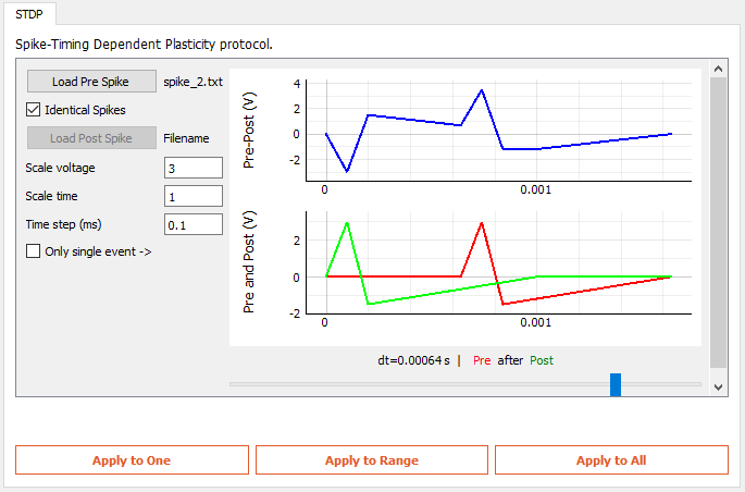
| Parameter | Description |
|---|---|
| Load Pre/Post Spike | Load a voltage series text file which
defines the pre- and post-synaptic pulses. This is a comma separated
text file with (voltage (V), time (s)) pairs, one per line.
The last point MUST be of zero amplitude (0 V). |
| Identical Spikes | When checked the post-synaptic spike will be identical to the pre-synaptic. |
| Scale voltage/time | Scale all pre- and post-synaptic spikes in amplitude and duration. |
| Time step (ms) | Sets a time step which is used when iterating through STDP events. |
| Only single event | When checked, only the STDP waveform shown in the top right figure is applied, one time, when clicking the Apply to One button. |
For example in the figure above, pre- and post- spikes are identical,
and their maximum duration is 1 ms. Time step is set to 0.1 ms
(henceforth referred to as timeStep). By clicking on Apply to …, the experiment will proceed as
follows: First, the resulting waveform of Pre-Post with
dt = 0 s will be applied, followed by the resulting
waveform for dt = +timeStep, then for
dt = -timeStep, then for dt =+2 × timeStep,
then for dt = -2 × timeStep and so on, until
dt becomes greater than the duration of the longest spike
(in this case both pre- and post- are the same at 1 ms).
MultiBias is used to apply a voltage pulse to multiple active wordlines, or read current from multiple devices in parallel sharing the same bitline.
| Parameter | Description |
|---|---|
| Active Wordlines | Whitespace delimited active wordline addresses. |
| Active Bitline | Active wordline address. Only one bitline allowed. |
| WRITE amplitude (V) | Amplitude of the WRITE pulse. |
| WRITE pulse width (V) | Pulse width of the WRITE pulse. |
| READ voltage (V) | Voltage used for the READ operation. |
There are no Apply to … operations in MultiBias as it inherently requires more than one device to work. The user is instead presented with the WRITE and READ buttons.
WRITE: When pressed, the module will apply a voltage pulse (V) to the selected active wordlines. The active bitline is grounded, and all other inactive word- and bit-lines will receive V/2.
READ: When pressed, the module will apply the read voltage to the active wordlines, then read and display the current on the active bitline in the Current on Active Bitline entrybox. During this operation, all inactive word- and bit-lines are held at virtual-GND.
The WRITE operation consists of the following stages:
ConvergeToState allows the user the program a memristor to a user-defined resistive state. It employs an algorithm simiral to FormFinder to deliver programming pulse ramps so as to gradually shift the resistance of the device to the desired level. In contrast to FormFinder this is not limited to a specific low resistance. ConvergeToState will instead try to “guess” the correct polarity of by observing the transient response of the resistance and will switch polarities if current resistance diverges away from the target. In order to avoid never-ending loops the number of possible reversals is limited to five (5).
| Parameter | Description |
|---|---|
| Target R (Ω) | Desired resistive level. |
| Rt tolerance (%) | Sets the target resistance tolerance. If current resistance is within the specified percentage of the target the algorithm terminates. |
| Initial polarity | Selects the initial voltage polarity. This can be a useful hint to the algorithm to avoid unnecessary polarity switches. |
| Ro tolerance (%) | Sets the initial resistance tolerance. Any ΔR below the specified value (in % of the initial) is not registered as deviation from the initial state. |
| PW min/step/max (ms/%/ms) | Programming pulse width characteristics. Before switching voltage amplitudes the system will increase the pulse width in % of the minimum until the maximum value has been reached. |
| Voltage min/step/max (V) | Programming amplitude characteristics. The system will scan from min to max. Once max has been reached the algorithm will terminate. |
| Interpulse (ms) | Interval between two consecutive pulses. |
| Pulses | Number of pulses per programming step. |
Tag: CTS. CovergeToState follows the
standard CTS_{s,i,e} format.
ChronoAmperometry measures the current and resistance of a device continuously while it is being kept under bias.
| Parameter | Description |
|---|---|
| Bias (V) | Applied voltage bias. |
| Bias duration (ms) | Duration of the applied pulse. |
| Number of reads | Times the device will be sampled while under bias (min: 2). |
Tag: CRA. ChronoAmperometry follows the
standard CRA_{s,i,e} format.
MultiStateSeeker is used to assess multiple stable resistive states on devices that exhibit analogue behaviour. It combines the polarity inference ability of the SwitchSeeker for polarity inference with additional code to switch the device to progressively lower or higher non-volatile states by programming it with controlled voltage pulses.
MultiStateSeeker consists of three phases that can be applied on an unknown device so as to assess the number of available states within a user-programmable tolerance threshold. Phase I essentially determines the sensitivity of the device to the polarity of the applied bias, not unlike to how SwitchSeeker does. Then, on Phase II, the device is driven to a low (or high resistive) state that is stable enough to be regarded as its “initial” state. The baseline criterion is either a linear fit or a t-test. This is, finally, followed by Phase III where the actual state assessment is performed. Using the polarity extracted from phase I a programming pulse is applied followed by two sets of READ pulse trains separated by a user-defined short-term retention interval. If current state is clearly separated by the previous by up to 9σ then the state is registered. Otherwise the number of pulses and subsequently the amplitude is increased until it does. Once a maximum voltage has been reached the measurement terminates.
The third phase of MultiStateSeeker presents a clickable entry (MultiState Calculation) in the Device History panel that displays a summary of calculated states.
Parameters of Phase I
The user parameters in Phase I follow the same semantics as those in SwitchSeeker.
Parameters of Phase II
| Parameter | Description |
|---|---|
| Pulse voltage (V) | Bias used to drive device to its baseline state. |
| Pulse width (ms) | Pulse width of pulse. |
| State mode | Can be either As calculated to use the polarity inferred from Phase I or Inverse polarity for the opposite value. |
| Stability test | The type of test to be used to evaluate stability of baseline; either Linear or T-test. |
| Max time (s) | Timeout for above test. |
| Tolerance or t-metric (%/-) | Stability criterion for linear fit and t-test respectively. |
Parameters of Phase III
| Parameter | Description |
|---|---|
| Mode | Parameter to sweep for assessment; can be either voltage sweep, pulse width sweep or programming sweep. |
| Reads | Number of pulses in READ train. Two READ trains separated by the retention interval (see below) will be applied after each programming step. |
| Max. programming pulses | The maximum number of programming pulses to use to switch the state of the device. Only available in voltage and pulse width modes. |
| Voltage bias (V) | Voltage bias to be applied for programming. Only available in pulse width and programming modes. |
| Voltage/PW/Pulses min/step/max | The sweep parameters depending on the active mode. Voltages in V; pulse widths in ms. |
| Interpulse (ms) | Interval between consecutive programming pulses. |
| Retention time (ms or s) | Delay between consecutive READ trains. |
| Std. deviations | Number of standard deviations that are required to separate consecutive resistive states (1σ: very dense states → 9σ: very coarse states) |
| Monotonicity | How the algorithm should treat resistance reversals (e.g. resistance decreases when the overall trend is increasing). Stop on reversal: stops immediately; Move to next step: apply the next pulse in sequence; Ignore: do nothing. |

Tag: MSS1 to MSS3 for each
respective state. Each one follows the standard
MSSX_{s,i,e} format.
SuperMode allows users to create chains of measurement modules to better fit your characterisation procedures. Instead of applying consecutive different pulsing modules by hand, simply create an experiment chain with full flexibility. The module can be found as a bold entry in the drop-down list on the Advanced Modules Panel.
The left-hand side column contains the available modules built in the platform, along with basic ones such as time delay (Delay), single voltage pulse and single READ operation. Furthermore, Start Loop and End Loop indicators can be utilised as well.
You can drag-and-drop your required modules onto the next column on the right (the chain column), between the blue Start and End markers. Rearrange them also by drag-and-drop, and discard unwanted ones by dropping them outside the chain column. When applying such an experiment chain to your devices, the instructions will be executed from top to bottom (Start to End).
Double click on a positioned module in the chain column to modify the procedure parameters. The selected module will be highlighted in the chain column. Double click on the Start Loop indicator to set the number of repetitions of the block contained. Nested loops are possible, and the system will check the order of the Start Loop and End Loop indicators for consistency before starting an experiment.
You can Save and later Load measurement chains via the corresponding buttons. The Clear button will delete all entries from the chain column.
[1] A. Serb, et. al. “Unsupervised learning in probabilistic neural networks with multi-state metal-oxide memristive synapses”, Nature Communications, 2016
[2] I. Gupta, et. al. “Real-time encoding and compression of neuronal spikes by metal-oxide memristors”, Nature Communications, 2016
[3] R. Berdan, et. al. “A μController-based system for interfacing selectorless RRAM crossbar arrays”, IEEE Transactions on Electron Devices, 62(7), 2190—2196, 2015
[4] R. Berdan, et. al. “Emulating short-term synaptic dynamics with memristive devices”, Scientific Reports, 6, 10.1038, 2016
In the case when the ArC ONE® board does not connect to the ArC GUI, try the following:
In the case when the ArC GUI does not receive correct data from the ArC board, save your data, reset the mBED and restart the GUI.